
We recently added this machine to the Fabrication Division to improve thru put and to add to our capabilities.

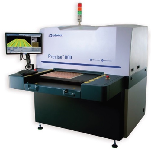
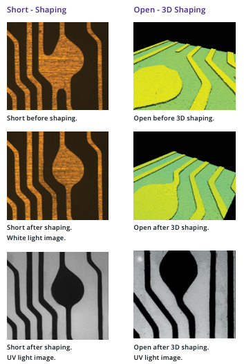
KLA's automated optical shaping (AOS) systems enable manufacturers to achieve high-speed, quality shaping of both opens and shorts that are identified along the PCB and IC substrate production line. As either an alternative to manual repair which often damages adjacent conductors and laminate, or for shaping fine lines on panels designated for scrap because they can’t be repaired manually, KLA's AOS solutions provide high-quality shaping, with minimum damage to the surrounding area for all main PCB applications including advanced high-density interconnects (HDI), IC substrates (ICS), multi-layer boards (MLB), flex PCBs and more. KLA's AOS solutions enable PCB and IC substrate manufacturers to increase yield and achieve significant cost savings by reducing their need to scrap panels of the most advanced, complex, fine-line PCBs, which in the past were beyond salvage.
Added: July 2026