 Our Advanced Microelectronics group now offers advanced microelectronics assembly and packaging services, process development, and low to medium-volume production for high-reliability applications. Utilizing our new state-of-the-art equipment and our 45+ years of process expertise, we enable customers to transition from prototype to low-volume production seamlessly.
Services to meet your advanced assembly and packaging needs:
|
|
 Access to advanced packaging as a service, with no long-term commitments. This allows companies to conduct low-risk experiments, process development, and accelerate the time to market without having to purchase expensive capital equipment.
|
|
| EQUIPMENT | SPECIFICATION | CAPABILITY |
| TPT HB-16 Wire Bonder |
0.7 mil to 3.0 mil (17-75um) round wire (wedge or ball) |
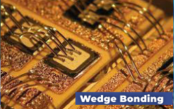
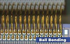
Gold and Aluminum Wedge Bonding as well as Gold Ball Bonding and Bumping |
| Tresky T-5300 Die Bonder | 1um placement accuracy (application dependent) 20g to 4kg bond force |
3D packaging of MEMS, VCSEL, Photonics, etc. Epoxy or eutectic die attach Flip-chip attach Epoxy dispense or pin transfer |
| Keyence VHX 7000N Digital Microscope | 20x to 2,000x zoom optics +/- 60 degree viewing angle Coaxial, Oblique, and back-lit illumination Depth composition Image stitching |
Sub-micron resolution images |
| XYZTEC Condor Sigma Pull/Shear Tester | Tests from 1 gram to 200 kg force 24-bit resolution 6 Sensors in Rotating Turret |
Fine Wire Pull Test (Destructive and Non-Destructive). Ribbon Pull Test (Destructive and Non-Destructive). Die Shear Test Automatic Testing Capable |
Search Tags:


